Shop : Review copy
Shop
Review copy
45,80 €ISBN 978-3-8440-7716-2Softcover152 pages76 figures225 g21 x 14,8 cmEnglishThesis
December 2020
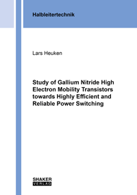
Lars Heuken
Study of Gallium Nitride High Electron Mobility Transistors towards Highly Efficient and Reliable Power Switching
In this work, the engineering challenges of the lateral GaN HEMT for power applications are addressed with the aim of making the GaN HEMT more reliable and efficient. The analysis is focused on the buffer layer, which defines the blocking voltage, on trapping effects in the buffer and on the device surface as well as on time-dependent reliability phenomena. To achieve high blocking voltages a homoepitaxially grown buffer with a low dislocation density is analyzed and different conduction mechanisms and activation energies of vertical buffer leakage current are found. Trapping on the device surface is experimentally verified by a test-transistor with multiple sensing gates, showing a lateral distribution of surface trapping with an extension of up to 600 nm from the main gate, enabling the quantification of trapped electrons. To increase the blocking voltage of the transistor, the buffer layer providing insulation of the transistor in the off-state is optimized by introducing a super-lattice (SL) buffer consisting of periodic repetitive C-doped AlN/AlGaN layers instead of a conventional C-doped GaN buffer. The developed growth conditions provide lower leakage, higher breakdown voltage and lower trapping than the conventional buffer structure. The SL buffer shows time-dependent degradation, which is superior to the degradation in the conventional concept and is related to a higher crystal quality. The role of C-compensation is identified to have a key influence on the expected device-lifetime, which is explained by the accelerated degradation due to the presence of defects and impurities in undoped or mildly doped buffers. To expand the validity of the results to large wafer sizes the distribution of transistor parameters across full 150 mm GaN/Si wafers is analyzed.
Keywords: Gallium Nitride; Power Electronics; GaN; GaN HEMT; Power Transistor
Shaker Verlag GmbH
Am Langen Graben 15a
52353 Düren
Germany
Am Langen Graben 15a
52353 Düren
Germany
Mon. - Thurs. 8:00 a.m. to 4:00 p.m.
Fri. 8:00 a.m. to 3:00 p.m.
Fri. 8:00 a.m. to 3:00 p.m.
Contact us. We will be happy to help you.


